Sunday, November 15, 2009

EARTH LEAKAGE CURRENT DETECTOR ICs

UTC M54123L LINEAR INTEGRATED CIRCUIT
EARTH LEAKAGE CURRENT DETECTOR


FUNCTION
The UTC M54123L circuit for the amplifying parts of earth leakage circuit breaker consists of differential amplifier, latch circuit and voltage regulator. It is connected to the secondary side of the zero current transformer (ZCT) which detects leakage current in the both input of the differential amplifier. Signals amplified by differential amplifier are integrated by an external capacitor, and connects to the input terminal of latch circuit with output suitable for the characteristics of high- speed earth leakage circuit breaker. Latch circuit keeps low in the output till the input voltage reaches the fixed level, and output becomes high when the leakage current more than fixed flows.
It drives a thyristor connected to the output terminal of latch circuit.

FEATURES*Suitable for JIS C 8371
*Good temperature characteristics of input sensitivity
current
*High input sensitivity (VT=6.1mV Typ.)
*Low external component count
*High noise and surge-proof
*Low power dissipation (Pd=5mW Typ.) and may be
used both as 100V and 200V.
*Wide temperature range (Ta=-20~+80°C)

Datasheethttp://www.unisonic.com.tw/datasheet/M54123L.pdf


KA2803B
Earth Leakage Detector
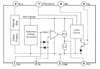


DescriptionThe KA2803B is designed for use in earth leakage circuit
interrupters, for stable operation of the AC line in breakers.
The input of the differential amplifier is connected to the
secondary coil of ZCT(Zero Current Transformer). The
amplified output of differential amplifier is integrated at
external capacitor to gain adequate time delay that is
specified in KSC4613. The level comparator generates high
level when earth leakage current is greater than the fixed
level.
Features
• Low Power Consumption PD =5mW, 100V/200V
• Built-in Voltage Regulator
• High Gain Differential Amplifier
• 0.4mA Output Current Pulse to Trigger SCR' S
• Low External Part Count
• DIP Package (8-DIP), High Packing Density
• High Noise Immunity, Large Surge Margin
• Super Temperature Characteristic of Input Sensitivity
• Wide Operating Temperature Range (TA = -25C ~
+80C)
• Operation from 12 to 20V Input

Datasheet
http://www.fairchildsemi.com/ds/KA%2FKA2803B.pdf


RV4141A
Low Power Ground Fault Interrupter


Description
The RV4141A is a low-power controller for AC receptacle
ground fault circuit interrupters. These devices detect
hazardous current paths to ground and ground to neutral
faults. The circuit interrupter then disconnects the load from
the line before a harmful or lethal shock occurs.
Internally, the RV4141A contains a diode rectifier, shunt
regulator, precision sense amplifier, current reference, time
delay circuit, and SCR driver.


Two sense transformers, SCR, solenoid, three resistors and
four capacitors complete the design of the basic circuit interrupter.
The simple layout and minimum component count
ensure ease of application and long term reliability.
Features not found in other GFCI controllers include a low
offset voltage sense amplifier eliminating the need for a
coupling capacitor between the sense transformer and sense
amplifier, and an internal rectifier to eliminate high voltage
rectifying diodes.


The RV4141A is powered only during the positive half
period of the line voltage, but can sense current faults independent
of its phase relative to the line voltage. The gate of
the SCR is driven only during the positive half cycle of the
line voltage.
Features
• Powered from the AC line
• Built-in rectifier
• Direct interface to SCR
• 500 μA quiescent current
• Precision sense amplifier
• Adjustable time delay
• Minimum external components
• Meets UL 943 requirements
• For use with 110V or 220V systems
• Available in an 8-pin SOIC package


Datasheethttp://www.fairchildsemi.com/ds/RV%2FRV4141A.pdf

Saturday, November 7, 2009

CAN BUS Driver IC

High-Speed CAN Transceiver
MCP2551
The MCP2551 is a high-speed CAN, fault-tolerant
device that serves as the interface between a CAN protocol
controller and the physical bus. The MCP2551
provides differential transmit and receive capability for
the CAN protocol controller and is fully compatible with
the ISO-11898 standard, including 24V requirements. It
will operate at speeds of up to 1 Mb/s.
Typically, each node in a CAN system must have a
device to convert the digital signals generated by a CAN
controller to signals suitable for transmission over the
bus cabling (differential output). It also provides a buffer
between the CAN controller and the high-voltage spikes
that can be generated on the CAN bus by outside
sources (EMI, ESD, electrical transients, etc.).

Features
• Supports 1 Mb/s operation
• Implements ISO-11898 standard physical layer
requirements
• Suitable for 12V and 24V systems
• Externally-controlled slope for reduced RFI
emissions
• Detection of ground fault (permanent dominant)
on TXD input
• Power-on reset and voltage brown-out protection
• An unpowered node or brown-out event will not
disturb the CAN bus
• Low current standby operation
• Protection against damage due to short-circuit
conditions (positive or negative battery voltage)
• Protection against high-voltage transients
• Automatic thermal shutdown protection
• Up to 112 nodes can be connected
• High noise immunity due to differential bus
implementation
• Temperature ranges:
- Industrial (I): -40°C to +85°C
- Extended (E): -40°C to +125°C
datasheet pdfhttp://ww1.microchip.com/downloads/en/DeviceDoc/21667d.pdf
Stand-Alone CAN Controller With SPI™ Interface
MCP2515
Description

Microchip Technology’s MCP2515 is a stand-alone
Controller Area Network (CAN) controller that implements
the CAN specification, version 2.0B. It is capable
of transmitting and receiving both standard and
extended data and remote frames. The MCP2515 has
two acceptance masks and six acceptance filters that
are used to filter out unwanted messages, thereby
reducing the host MCUs overhead. The MCP2515
interfaces with microcontrollers (MCUs) via an industry
standard Serial Peripheral Interface (SPI).
Features
• Implements CAN V2.0B at 1 Mb/s:
- 0 – 8 byte length in the data field
- Standard and extended data and remote
frames
• Receive buffers, masks and filters:
- Two receive buffers with prioritized message
storage
- Six 29-bit filters
- Two 29-bit masks
• Data byte filtering on the first two data bytes
(applies to standard data frames)
• Three transmit buffers with prioritizaton and abort
features
• High-speed SPI™ Interface (10 MHz):
- SPI modes 0,0 and 1,1
• One-shot mode ensures message transmission is
attempted only one time
• Clock out pin with programmable prescaler:
- Can be used as a clock source for other
device(s)
• Start-of-Frame (SOF) signal is available for
monitoring the SOF signal:
- Can be used for time-slot-based protocols
and/or bus diagnostics to detect early bus
degredation
• Interrupt output pin with selectable enables
• Buffer Full output pins configurable as:
- Interrupt output for each receive buffer
- General purpose output
• Request-to-Send (RTS) input pins individually
configurable as:
- Control pins to request transmission for each
transmit buffer
- General purpose inputs
• Low-power CMOS technology:
- Operates from 2.7V – 5.5V
- 5 mA active current (typical)
- 1 µA standby current (typical) (Sleep mode)
• Temperature ranges supported:
- Industrial (I): -40°C to +85°C
- Extended (E): -40°C to +125°C
datasheet pdfhttp://ww1.microchip.com/downloads/en/DeviceDoc/21801d.pdf
High speed CAN transceiver
TJA1040
GENERAL DESCRIPTION

The TJA1040 is the interface between the Controller Area
Network (CAN) protocol controller and the physical bus.
It is primarily intended for high speed applications, up to
1 MBaud, in passenger cars. The device provides
differential transmit capability to the bus and differential
receive capability to the CAN controller.
The TJA1040 is the next step up from the TJA1050 high
speed CAN transceiver. Being pin compatible and offering
the same excellent EMC performance, the TJA1040 also

features:
- An ideal passive behaviour when supply voltage is off
- A very low-current standby mode with remote wake-up
capability via the bus.

This makes the TJA1040 an excellent choice in nodes
which can be in power-down or standby mode in partially
powered networks.

FEATURES
- Fully compatible with the ISO 11898 standard
- High speed (up to 1 MBaud)
- Very low-current standby mode with remote wake-up
capability via the bus
- Very low ElectroMagnetic Emission (EME)
- Differential receiver with high common-mode range for
ElectroMagnetic Immunity (EMI)
- Transceiver in unpowered state disengages from the
bus (zero load)
- Input levels compatible with 3.3 V and 5 V devices
- Voltage source for stabilizing the recessive bus level if
split termination is used (further improvement of EME)
- At least 110 nodes can be connected
- Transmit Data (TXD) dominant time-out function
- Bus pins protected against transients in automotive
environments
- Bus pins and pin SPLIT short-circuit proof to battery and
ground
- Thermally protected.

datasheet pdf
http://www.nxp.com/acrobat_download/datasheets/TJA1040_6.pdf
SN65HVD230
SN65HVD231
SN65HVD232
3.3-V CAN TRANSCEIVERS

DESCRIPTION

.
The SN65HVD230, SN65HVD231, and SN65HVD232 controller area network (CAN) transceivers are designed for use with the Texas Instruments TMS320Lx240x™; 3.3-V DSPs with CAN controllers, or with equivalent devices. They are intended for use in applications employing the CAN serial communication physical layer in accordance with the ISO 11898 standard. Each CAN transceiver is designed to provide differential transmit capability to the bus and differential receive capability to a CAN controller at speeds up to 1 Mbps.

Designed for operation in especially-harsh environments, these devices feature cross-wire protection, loss-of-ground and overvoltage protection, overtemperature protection, as well as wide common-mode range.

The transceiver interfaces the single-ended CAN controller with the differential CAN bus found in industrial,building automation, and automotive applications. It operates over a -2-V to 7-V common-mode range on the bus, and it can withstand common-mode transients of ±25 V.

On the SN65HVD230 and SN65HVD231, pin 8 provides three different modes of operation: high-speed, slope control, and low-power modes. The high-speed mode of operation is selected by connecting pin 8 to ground, allowing the transmitter output transistors to switch on and off as fast as possible with no limitation on the rise and fall slopes. The rise and fall slopes can be adjusted by connecting a resistor to ground at pin 8, since the slope is proportional to the pin's output current. This slope control is implemented with external resistor values of 10 kΩ, to achieve a 15-V/s slew rate, to 100 kΩ, to achieve a 2-V/s slew rate. See the Application Information
section of this data sheet.

FEATURES
- Operates With a 3.3-V Supply
- Low Power Replacement for the PCA82C250 Footprint
- Bus/Pin ESD Protection Exceeds 16 kV HBM
- High Input Impedance Allows for 120 Nodes on
- Controlled Driver Output Transition Times for
Improved Signal Quality on the SN65HVD230
and SN65HVD231
- Unpowered Node Does Not Disturb the Bus
- Compatible With the Requirements of the ISO
11898 Standard
- Low-Current SN65HVD230 Standby Mode
370 A Typical
- Low-Current SN65HVD231 Sleep Mode 40 nA
Typical
- Designed for Signaling Rates(1) up to 1
Megabit/Second (Mbps)
- Thermal Shutdown Protection
- Open-Circuit Fail-Safe Design
- Glitch-Free Power-Up and Power-Down
Protection for Hot-Plugging Applications
datasheet pdf
http://focus.ti.com/lit/ds/symlink/sn65hvd230.pdf

PCA82C250
CAN controller interface
General description

The PCA82C250 is the interface between a CAN protocol controller and the physical bus.The device provides differential transmit capability to the bus and differential receive capability to the CAN controller.

Features- Fully compatible with the “ISO 11898” standard
- High speed (up to 1 MBd)
- Bus lines protected against transients in an automotive environment
- Slope control to reduce Radio Frequency Interference (RFI)
- Differential receiver with wide common-mode range for high immunity against
ElectroMagnetic Interference (EMI)
- Thermally protected
- Short-circuit proof to battery and ground
- Low-current Standby mode
- An unpowered node does not disturb the bus lines
- At least 110 nodes can be connected

datasheet pdf
http://www.nxp.com/acrobat_download/datasheets/PCA82C250_6.pdf

Sunday, November 1, 2009

Poly-Phase Energy Metering IC

ADE7758
Poly Phase Multifunction Energy Metering IC with Per Phase Information

GENERAL DESCRIPTION
The ADE77581 is a high accuracy, 3-phase electrical energy measurement IC with a serial interface and two pulse outputs. The ADE7758 incorporates second-order Σ-Δ ADCs, a digital integrator, reference circuitry, a temperature sensor, and all the signal processing required to perform active, reactive, and apparent energy measurement and rms calculations.
The ADE7758 is suitable to measure active, reactive, and apparent energy in various 3-phase configurations, such as WYE or DELTA services, with both three and four wires. The ADE7758 provides system calibration features for each phase, that is, rms offset correction, phase calibration, and power calibration. The APCF logic output gives active power information, and the VARCF logic output provides instantaneous reactive or apparent power information

FEATURES
Highly accurate; supports IEC 60687, IEC 61036, IEC 61268, IEC 62053-21, IEC 62053-22, and IEC 62053-23

Compatible with 3-phase/3-wire, 3-phase/4-wire, and other 3-phase services

Less than 0.1% active energy error over a dynamic range of 1000 to 1 at 25ฐC

Supplies active/reactive/apparent energy, voltage rms, current rms, and sampled waveform data

Two pulse outputs, one for active power and the other selectable between reactive and apparent power with programmable frequency

Digital power, phase, and rms offset calibration

On-chip, user-programmable thresholds for line voltage SAG and overvoltage detections

An on-chip, digital integrator enables direct interface-to-current sensors with di/dt output

A PGA in the current channel allows direct interface to shunts and current transformers

An SPIฎ-compatible serial interface with IRQ

Proprietary ADCs and DSP provide high accuracy over large variations in environmental conditions and time

Reference 2.4 V (drift 30 ppm/ฐC typical) with external overdrive capability

Single 5 V supply, low power (70 mW typical)

http://www.analog.com/static/imported-files/data_sheets/ADE7758.pdf

MCP3909
Energy Metering IC with SPI Interface and Active Power Pulse Output


Description
The MCP3909 device is an energy-metering IC
designed to support the IEC 62053 international
metering standard specification. It supplies a frequency
output proportional to the average active real power,
with simultaneous serial access to ADC channels and
multiplier output data. This output waveform data is
available at up to 14 kHz with 16-bit ADC output and
20-bit multiplier output words. The 16-bit, delta-sigma
ADCs allow for a wide range of IB and IMAX currents
and/or small shunt

Features
• Supports IEC 62053 International Energy
Metering Specification and legacy IEC 1036/
61036/687 Specifications
• Digital waveform data access through SPI
interface
- 16-bit Dual ADC output data words
- 20-bit Multiplier output data word
• Dual functionality pins support serial interface
access and simultaneous Active Power Pulse
Output
• Two 16-bit second order delta-sigma
Analog-to-Digital Converters (ADCs) with multi-bit
DAC
- 81 dB SINAD (typ.) both channels
• 0.1% typical active energy measurement error
over 1000:1 dynamic range
• PGA for small signal inputs supports low value
shunt current sensor
• Ultra-low drift on-chip reference:
15 ppm/°C (typical)
• Direct drive for electromagnetic mechanical
counter and two-phase stepper motors
• Low IDD of 4 mA (maximum)
• Tamper output pin for negative power indication
• Industrial Temperature Range: -40°C to +85°C

http://ww1.microchip.com/downloads/en/DeviceDoc/22025b.pdf

GENERAL DESCRIPTION
The ADE7752 is a high accuracy polyphase electrical energy measurement IC.

The ADE7752A is a pin-to-pin compatible low power version of ADE7752. The functions of ADE7752 and ADE7752A are the same. Both products are referred to in the text of this data sheet as ADE7752. The part specifications surpass the accuracy requirements as quoted in the IEC62053-2x standard. The only analog circuitry used in the ADE7752 is in the analog-to-digital converters (ADCs) and reference circuit. All other signal processing (such as multi-plication, filtering, and summation) is carried out in the digital domain. This approach provides superior stability and accuracy over extremes in environmental conditions and over time.
FEATURES
High accuracy, supports 50 Hz/60 Hz IEC62053-2x

Less than 0.1% error over a dynamic range of 500 to 1

Compatible with 3-phase/3-wire delta and 3-phase/4-wire Wye configurations

The ADE77521 supplies average real power on frequency outputs F1 and F2

High frequency output CF is intended for calibration and supplies instantaneous real power

Logic output REVP indicates a potential miswiring or negative power for each phase Direct drive for electromechanical counters and 2-phase stepper motors (F1 and F2)

Proprietary ADCs and DSP provide high accuracy over large variations in environmental conditions and time On-chip power supply monitoring

On-chip creep protection (no load threshold) On-chip reference 2.4 V ฑ8% (20 ppm/ฐC typical) with external overdrive capability

Single 5 V supply, low power 60 mW typical: ADE7752 30 mW typical: ADE7752A

Low cost CMOS process

http://www.analog.com/static/imported-files/data_sheets/ADE7752_7752A.pdf